Semiconductor Lithography Optics (Photolithography) in Hydrogen
[vc_row][vc_column][vc_empty_space][vc_row_inner][vc_column_inner][title title=”Semiconductor Lithography Optics (Photolithography) in Hydrogen” title_color=”#ffffff” title_bg_color=”#1e73be” title_padding=”20px 0px 20px 20px” line=”no” animate=”yes”][/vc_column_inner][/vc_row_inner][vc_row_inner][vc_column_inner width=”1/2″][vc_column_text]
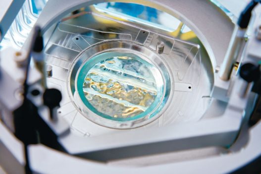
Today’s semiconductor manufacturing uses Photolithography in the microfabrication process to pattern parts of a thin film or the bulk of a substrate.
It uses extreme ultra violet light to transfer complex geometric patterns from a photomask to a light-sensitive chemical “photoresist” on the substrate. A series of chemical treatments then either engraves the exposure pattern into, or enables deposition of a new material in the desired pattern upon, the material underneath the photo resist.
The complex optical systems used in lithography systems are critical to shrinking the size of microchips. One way to pack more, smaller circuits onto a semiconductor is to use light with a shorter wavelength, such as ultra-violet light. At such narrow wavelengths, regular air would distort the beam path and that is why they are often operated in atmospheres of hydrogen or other gas blends.
[/vc_column_text][vc_column_text]When hydrogen atmospheres are used for lithography optics, that hydrogen must be very pure. For monitoring and validating hydrogen quality, engineers can use the parts-per-billion levels of detection found in the HEMS analyzer. The HEMS instrument can continuously sample the hydrogen quality directly from feed lines, eliminating the need for offline measurements performed by scientists in a laboratory.[/vc_column_text][/vc_column_inner][vc_column_inner width=”1/2″][vc_single_image source=”featured_image” img_size=”large” add_caption=”yes”][vc_btn title=”HEMS-M Product Specifications” style=”3d” color=”info” size=”sm” link=”url:http%3A%2F%2Fpowerandenergy.com%2Fpdfs%2Fhems-m-data-sheet.pdf|title:HEMS-M%20Product%20Specifications|target:%20_blank|rel:nofollow”][vc_btn title=”Contact Sales” style=”3d” color=”warning” size=”sm” link=”url:http%3A%2F%2Fwww.powerandenergy.com%2Fcontact-us%2F|title:Contact%20Sales||”][vc_btn title=”Back to Product Page (HEMS)” style=”3d” size=”sm” i_icon_fontawesome=”fa fa-hand-o-left” add_icon=”true” link=”url:http%3A%2F%2Fwww.ep.to%2Fhydrogen-extraction-products%2Fhydrogen-purity-analyzers%2F|title:Back%20to%20Product%20Page%20(HEMS)||”][/vc_column_inner][/vc_row_inner][vc_column_text]
Product Applications
[/vc_column_text][vc_row_inner][vc_column_inner][vc_basic_grid post_type=”post” max_items=”4″ style=”load-more” element_width=”3″ orderby=”ID” btn_style=”3d” grid_id=”vc_gid:1540984510535-086b5bf0-89d7-9″][/vc_column_inner][/vc_row_inner][/vc_column][/vc_row]